Considerations for custom burn-in solution
Starting with thin (nanometer range), round wafers of silicon crystal, the fabrication process involves building a succession of layers of materials and geometries to produce thousands of electronic devices at tiny sizes, which together function as integrated circuits (ICs). The devices which now occupy the surface of a one-inch square IC would have occupied the better part of a medium-sized room 20 years ago, when all these devices (transistors, resistors, capacitors, and so on) were only available as discreet units. Because of the inherent nature of wafer processing, the reliability of individual silicon die is verified by another process called “burn-in process”. Burn-in is the process by which components of a system are exercised prior to being placed in service (and often, prior to the system being completely assembled from those components). As the number of transistors and the total amount of circuitry on a chip increases, the potential for a defect increases, leading to immediate or future failures. Because of the complexity of the processes used during fabrication, some chips may pass initial QC test but fail after a short time. These devices must be identified and scrapped before assembly. Burn-in test lets the manufacturer identify these potential faulty devices and remove them from being used.
Burn-in exposes an electrical device at an elevated temperature for a specified number of hours, generally with bias and an electrical load (Bias is the application of an external DC voltage to set the upper and lower operating limits of a device) applied. This is done in an attempt to stress all elements of the device at maximum rated operating conditions in order to reveal all stress and time dependent failure mode
A typical ICs life is exemplified by bath tub curve. Because of inherent nature of IC manufacturing processes, a few percent of ICs fail very early in their life and the failure is very minimal during its life time and then failure percentage goes up at end of IC life. Burn-in tests are conducted to screen those early failures. Typical burn-in test includes testing IC device at 125 degree C for 8 hours. If the IC passes this test which means it is ready for primetime. Typically a socket mounted on burn-in board capable of applying proper electrical load is used in burn-in test. An IC socket is an electromechanical device that provides a pluggable interface between an IC package and a burn-in system circuit board. This interface must be accomplished with maximum repeatability and minimal effect on circuitry. Providing for a removable interface is a major reason for using a socket and may be required for ease of assembly, and cost savings. The socket is attached to the PCB, while the IC device can be inserted into or removed from the socket without disturbing the connections to the PCB. This allows the IC to function as it is soldered onto the PCB but also be replaced by another IC or multiple IC’s. Typical socket requirements are high temperature and high insertion/extraction cycles. Since millions of manufactured IC’s go through this burn-in test, more sockets are needed which drives the socket cost down to low. Socket technology using molded housing and low cost stamped contact satisfies burn-in test market.
For standard packages, low cost burn-in sockets are available off-the-shelf. They are constructed using molded housing and stamped contacts. Both molding and stamping are high volume manufacturing operations which need high initial cost for tooling. Socket manufacturers invest tooling cost for generic packages and amortize the cost over tens of thousands of sockets. When it comes to custom packages, it is not profitable to invest initially and amortize over tens of thousands of sockets because the test need will be only for few hundred sockets.
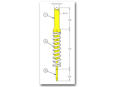
- 1. Top plunger
- 2. Bottom plunger
- 3. Gold plated stainless steel spring
Ironwood Electronics developed a process to address this unique problem using a stamped spring pin contact technology. Stamped spring pin contact (figure 1) is a stamped contact with outside spring as well as inside leaf spring that provides a robust solution for Burn-in & Test applications. Contact technology has 3 part system which includes top plunger, bottom plunger and a spring. There is no barrel. The Beryllium Copper plungers are stamped and assembled to a stainless steel spring in an automated system to enable lowest resistance path for electrical signal to travel.
Typical specifications for the Stamped pogo pin contact technology include:
- 4GHz – 31.7GHz bandwidth @-1dB
- Contact resistance under 15mOhm
- Self inductance 0.88 – 0.95nH
- Capacitance under 0.3pF
- Operating temperature range -55C to +180C
- Insertion/Extraction life over 500,000 cycles
- Current rating at 80C temperature rise is 4 to 8 Amps per pin
These contact pin specifications meet burn-in test requirements very well. These stamped spring pin can be arranged in any configuration to address challenges of unique package variations.
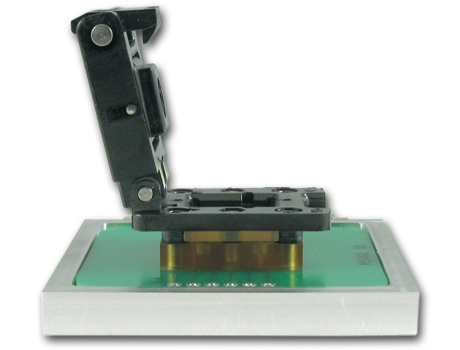
The second biggest hurdle is socket housing, specifically molded housing versus machined housing and its cost advantages. Ironwood Electronics have developed a unique process to manufacture custom molded housing for low volumes at competitive cost structure. Typical socket housing (figure 2) includes a lid, body, latch and a compression mechanism. Latch can be universal for all socket types. A unique latch design was developed and mold tooling was established. Since the latch is universal and it can be used in various sockets, cost per latch is very minimal for each socket. Socket lid can be universal to an extent which means 3 to 4 sizes can accommodate all package variations. By this way cost is distributed over few socket designs as opposed to each design. Socket body can be universal as well provided an individual IC guide is used for each unique package. Precise IC guide can be manufactured using laser machining and is very cost effective. Springs and other hardware used are standard off-the-shelf-components which add very miniscule cost. By this way, Ironwood Electronics provide custom burn-in socket solution at a very competitive price structure for end users that enables overall lower cost of test.
Typically the first step in procuring custom burn-in socket is that customer communicates their device specification to Ironwood Electronics. An application engineer will be assigned for this request who works with your design engineer and produce a custom socket drawing that shows footprint information. A proposal will be sent to the customer after acceptance of the custom socket drawing. We provide various options such as first article, delivery schedule and quantity price break downs. At the start of the project, our application and design engineering team will work on your project and keep customer updated on schedules and project milestones.
For your custom packages, please contact 800-404-0204 or email info@ironwoodelectronics.com