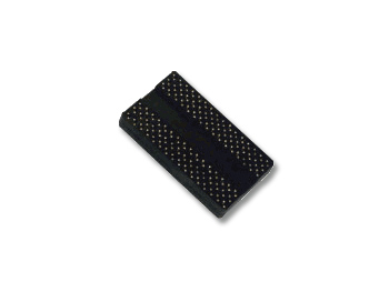
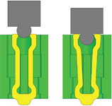
Grypper


- Package-size PCB footprint: Since the PCB footprint of Grypper is identical to or smaller than the IC package, only one PCB design is required, enabling a seamless transition from test and validation through production and reducing overall cost of test
- No lid required: The package snaps directly without a lid, enabling easy probing, scoping and troubleshooting the topside of the device
- Excellent signal performance: A short signal path achieves low inductance and low insertion loss, providing a nearly invisible electrical connection

Request For Quote or call us at 1-800-404-0204.