BGA Sockets
Ironwood has the most comprehensive collection of BGA (Ball Grid Array) sockets that can be used for prototype application, silicon validation, system development, thermal characterization, burn-in application, functional production test, etc.
BGA socket can be defined as an electromechanical device, which provides removable interface between IC package and system circuit board with minimal effect on signal integrity. BGA sockets for prototype applications, silicon validations, system development applications uses low cost elastomer contact technology.
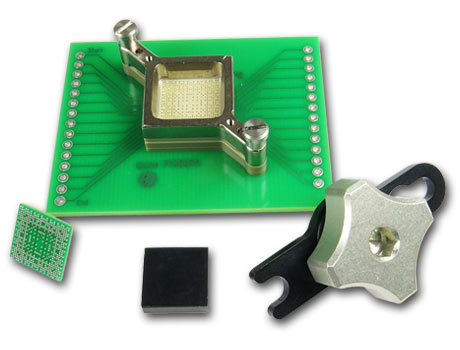
Figure 1 shows a BGA socket using embedded wire in elastomer (SG) contact technology. The SG elastomer consists of fine pitch matrix (0.05mm x 0.05mm) of gold plated wires (20 micron diameter), which are embedded at a 63-degree angle in a soft insulating sheet of silicone rubber.
Typical specifications for the SG interconnect include:
- 27 to >40 GHz Bandwidth
- 0.06 to 0.11nH Self Inductance
- 0.023 to 0.041nH Mutual Inductance
- 0.012 to 0.02pF Mutual Capacitance
- Less than 30 mOhms Contact Resistance
- -35C to +125C
- 0.2 to 2 Amps per pin
- 25-35 grams per pin
- 2000 to 3000 Insertions
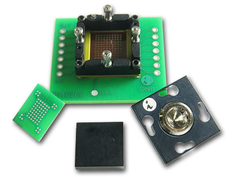
elastomer (SG) contact technology
SG Elastomer
The SG elastomer contact lasts for testing few thousand devices with occasional cleaning needed depending on the usage and the environment. The socket is constructed with shoulder screw and swivel lid which incorporates a quick insertion method so that IC’s can be changed out quickly. The socket is mounted on the target PCB with no soldering, and uses industry’s smallest footprint (only 2.5mm more on each side). To use, place the device inside the socket, place the compression plate and swivel the lid to close. Vertical force is applied using a torque tool via compression screw. Torque tool enhances the life of elastomer contact in terms of reliability and repeatability. The video shows torque applied on a BGA socket using a torque limited driver.
Torque Tool
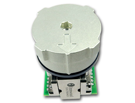
Alternatively torque tool can be integrated into the BGA socket design. Figure 2 shows such a BGA socket with torque indicating screw. These torque indicators are calibrated to precise torque needed for the specific BGA socket from the factory.
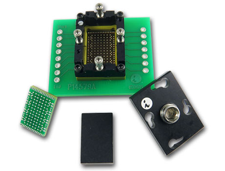
Some of the applications need data rate such as 50Gbps. General rule of thumb translates 50Gbps into 75GHz bandwidth. Ironwood’s GT sockets use innovative elastomer interconnect technology that delivers low signal loss (-1dB at 75GHz) and supports BGA packages with pitches down to 0.15mm. GT is a new elastomer technology that has silver particles held in a conductive column like buttons which are embedded in a non-conductive polymer substrate on a proper pitch that provides high compliance and extreme temperature ranges (-55C to +160C). Life cycle is very similar to SG elastomer. GT elastomer needs torque tool as well for vertical compression force application.
GT Elastomer
Example GT elastomer BGA socket is shown in Figure 3.
Typical specifications for the GT interconnect include:
- 94 GHz Bandwidth
- 0.04 to 0.06nH Self Inductance
- 0.003 to 0.024nH Mutual Inductance
- 0.006 to 0.012pF Mutual Capacitance
- Less than 30 mOhms Contact Resistance
- -55C to +160C
- 5 Amps per pin
- 50-80 grams per pin
- 1000 to 2000 Insertions
SBT BGA Sockets
When the applications demand thermal requirement, Ironwood’s BGA socket uses stamped spring pin (SBT) contact technology. SBT BGA sockets can be mounted on the same footprint as SG or GT BGA sockets. SBT BGA sockets simplify lab and evaluation applications due to low cost and better electrical/mechanical performance than conventional pogo pin sockets. SBT Contact is a stamped contact with outside spring as well as inside leaf spring that provides a robust solution for Burn-in & Test applications.
Typical specifications for the SBT interconnect include:
- 7 to 31.7 GHz Bandwidth
- 0.88 to 0.98nH Self Inductance
- 0.06 to 0.3nH Mutual Inductance
- 0.014 to 0.093pF Mutual Capacitance
- Less than 50 mOhms Contact Resistance
- -55C to +180C
- 4 to 8 Amps per pin
- 17 to 31 grams per pin
- 50,000 to 500,000 Insertions
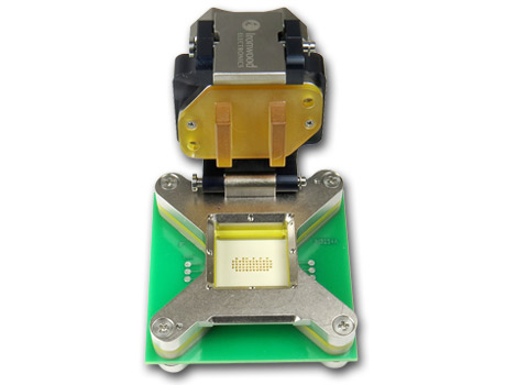
SBT BGA sockets are typically designed with clamshell lid for easy open and close. Compression plate is integrated to the clamshell lid. No torque tool is needed. When the force is applied by turning the compression screw, a built in stop position prevents from over compression. Example SBT BGA socket with clamshell lid is shown in Figure 4.
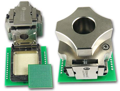
BGA Sockets with thermal access hole
A feature that is built into this BGA socket is thermal access hole. It is used for two reasons. One is to place a thermo couple from the top and access the case temperature of the BGA. The second reason is to use with thermal chamber where hot air is forced through the top. This will maintain case at specific temperature to verify the device is functioning properly at the temperature. Hot air from the top escapes out through the air flow channel designed in the compression plate of BGA socket.
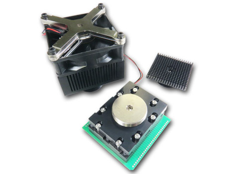
Many of the applications demand high power chips. In those scenarios, BGA sockets are designed with heat sink and fan which can dissipate up to 100 watts. Example BGA socket with heat sink and fan is shown in Figure 5. This BGA socket has a bracket on the top which has hex slot for torque application. This bracket allows to apply torque without removing fan every time BGA is inserted. BGA socket can use optional heat sink screw or regular compression screw based on the application requirement.
BGA Sockets with existing mounting holes
There are cases where customer has PCB made with top side components. In those situations, BGA socket can be designed with existing holes on the PCB. PCB gerber data is needed to determine the right set of mounting holes to be used in the BGA socket. Figure 6 shows a BGA socket designed with existing mounting hole and areas cleared for the top side components.
hole and areas cleared for the top side components
BGA Sockets with two mounting holes only
BGA sockets can be made using two mounting holes only. This enables customer to have more room for components and routing channel for PCB traces on the top layer. Figure 7 shows two mounting hole BGA socket using SBT contact technology.
BGA sockets with SBT contact for burn-in application
A typical BGA chip life is exemplified by bath tub curve. Because of inherent nature of BGA manufacturing processes, few percentage of BGAs fail very early in their life and the failure is very minimal during its life time and then failure percentage goes up at end of their life. Burn-in tests are conducted to screen those early failures. Typical burn-in test includes testing BGA device at 125C for 8 hrs. BGA sockets used for these applications have to be robust with no manual force application. Figure 8 shows a BGA socket with SBT contact for burn-in application. It also features a spring loaded lid. This means when the lid is closed, proper force is applied. This is necessary for burn-in application as millions of devices have to go through this phase for screening early failures.
SMP BGA Sockets
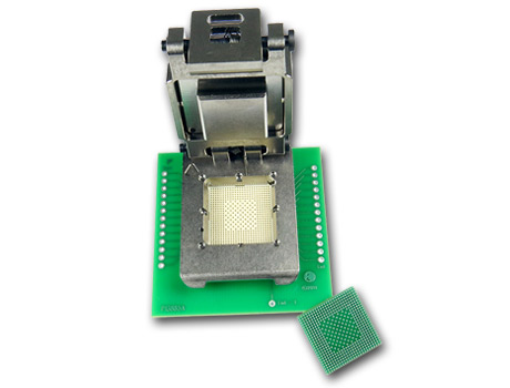
After passing burn-in test, these BGAs go through functional test which is often called production test. Since function is verified at this stage, bandwidth and current capacity requirements ranked high. This means a high speed BGA socket is needed to accomplish this phase of testing. Since millions of devices are being tested, higher the insertion/extraction cycle count, lower the overall cost of test is a must. This means BGA socket should test hundreds of thousands of devices. This unique situation calls for a high speed and high cycle count BGA socket. Ironwood’s SMP BGA socket uses silver ball matrix contact technology with a protective plunger matrix (a gold plated copper cylinder) that sits on top of the conductive columns. This plunger matrix protects the conductive column from contamination from various solder ball interfaces due to high cycle count. A quickly replaceable plunger matrix enables minimal downtime during final production test. Silver ball matrix elastomer accommodates high speed >40GHz. In addition to these electrical requirements, BGA socket design has to be compatible with handler which mechanically loads BGAs into the socket while the tester is performing functional verification. Figure 9 shows a SMP BGA socket with double latch lid for manual set up. Once the tester is set to test, the double latch lid is removed and handler starts loading devices as per programmed intervals.
Typical specifications for the SMP interconnect include:
- >40 GHz Bandwidth
- 0.1 to 0.14nH Self Inductance
- 0.017 to 0.031nH Mutual Inductance
- 0.004 to 0.01pF Mutual Capacitance
- Less than 30 mOhms Contact Resistance
- -55C to +155C
- 4 Amps per pin
- 50 to 80 grams per pin
- 500,000 Insertions
BGA sockets with insulation plate
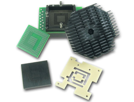
BGA sockets need vertical force which connects BGAs to elastomer or spring pins which in turn connects to the target PCB pads. Since the force applied varies due to pin count, pitch, contact technology used a back support plate called stiffener is always used in almost all of the BGA socket design. In most cases, the backside of target PCB contains capacitors and resistors. Since the stiffener plate cannot go on top of the components, a custom insulation plate with cavities milled for those capacitors and resistors has to be designed. The insulation plate sandwiches between the back support plate and the target PCB. Figure 10 shows an example BGA socket with insulation plate.
BGA sockets with backing plate
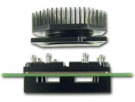
Alternatively, a five post back plate is used in the BGA socket wherein the post locations are predefined as keep out zone for the bottom side PCB. Figure 11 shows BGA socket with back plate that has protruded post location that allows capacitors and resistors to be populated in between the post location.
SMT Adapter Bases
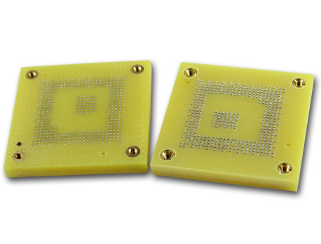
When through hole mounting is not possible on the target PCB for mechanically mounting BGA sockets, adapter bases are available that emulate the chips’s BGA footprint. This converts the BGA socket to an SMT component. The adapter bases are available for 0.5mm to 1.27mm pitch. SMT adapter bases are easily installed using standard flux and reflow techniques. After soldering down SMT adapter bases to the BGA pads on the target PCB, BGA sockets can be mechanically mounted to the adapter bases using hardware. Example SMT adapter base is shown in Figure 12.
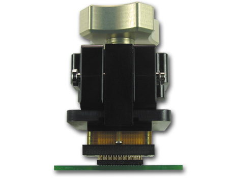
Stack Up SMT Adapters
SMT adapter bases have larger footprint than IC device due to the mounting hardware in the four corner and/or sides. When electrical design of the target PCB demands other passive components to be placed nearby the chip, SMT adapter bases with larger footprint cannot be used. Alternate solution is to lift up the adapter such that components can be placed closeby. In those scenarios, chip size SMT adapter (Giga-snaP product line) can be attached to target PCB using standard flux and reflow method and a through hole adapter can be used. Through hole adapters receive BGA sockets on the top side which has pins on the bottom side that can be plugged into the chip size SMT adapter to complete the connection. Example stack up is shown in Figure 13.
Epoxy mounted sockets
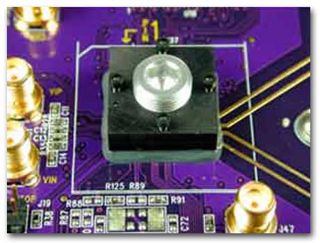
Both SMT adapter and SMT+ through hole adapter stack up adds signal length which means reduced signal speed. Some of the testing applications cannot withstand lower signal speed. In those situations, an epoxy mounted BGA socket is an option. While this creates a more or less permanent bonding of the socket to the PC Board, the socket is designed such that the contacting elements are replaceable should damage or excessive wear occur. These patented BGA sockets are simply mounted to the target PCB by an epoxy band around the perimeter. The socket is placed into position with a precision alignment tool and applying a ring of epoxy around the socket strongly holds it in place. There are special grooves on the socket wall for additional retention strength. The contactor can be easily replaced after hundreds of cycles. An example epoxy mounting procedure is shown in the linked document. Example epoxy mounted socket is shown in Figure 14.
Custom BGA sockets to accommodate rectangular body shapes, odd sizes, and devices with pitches down to 0.3mm can be developed in short lead time. BGA package specifications can vary widely between manufacturers. We have found that it is most effective for us to ask customers for information about the specific device to be tested in the BGA socket and then provide a quote. You can fill the form with required information or call us at 1-800-404-0204.