Solve component obsolescence problems with an Ironwood adapter and an alternate device. Adapters convert the pinout of an alternate device to maintain compatibility with an existing footprint – no need to redesign a new circuit board. Very often, these adapters (called Package Converters) are a simple 1:1 pin mapping from the new package to the old. Here are a few examples of package converters and how they can solve chip obsolescence issues.
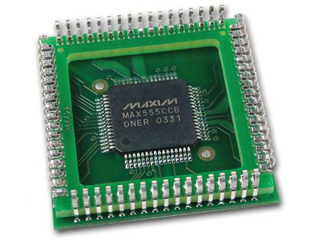
This QFP/PLCC package converter for a MAX555 device is ready to be surface mounted to a target board with a 68 pin PLCC land pattern to replace an obsolete PLCC device. Traces routed beneath the TQFP package maintain desired 50Ω transmission line impedance for optimum signal integrity while clock signals are routed as differential pairs to ensure a clean clock. Implementing these PCB features on a new target board requires significant design resources and manufacturing cost – producing these features on a small converter board proves cost efficient and allows seamless transition into the end-product without re-spinning the target board.
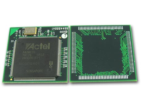
This custom package converter is used to replace an obsolete 128-pin PQFP ASIC with a 176-pin TQFP FPGA. The bottom side matches the footprint of the original PQFP for direct replacement. In addition to the TQFP, there is also a SMD Clock Oscillator and additional passive components. Solder columns are used to interface the package converter to the target board, accommodating overall height restrictions. Solder column technology is very similar to BGA assembly, but uses shaped solder instead of round solder balls.
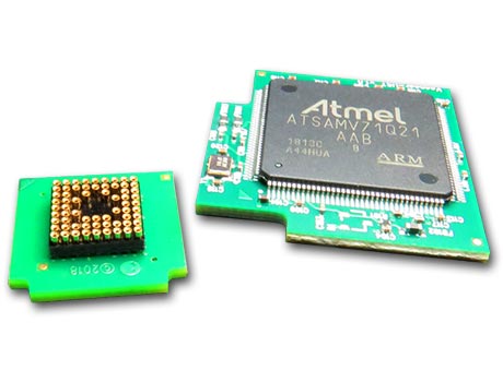
In this example, a pluggable 2-piece system is used where the original footprint is smaller than the new device. The lower adapter has 100 pin QFP solder column leads on the bottom side that are soldered to the existing footprint, with signals routed to an array of female pins on the top side for interconnect. A daughter card has an array of male pins on the bottom side, which mate with the female pin array on the bottom adapter. The daughter card has 144 QFP package with other passive components on the top side. The daughter card not only replaces the old device, but also upgrades the whole system with new functionality.
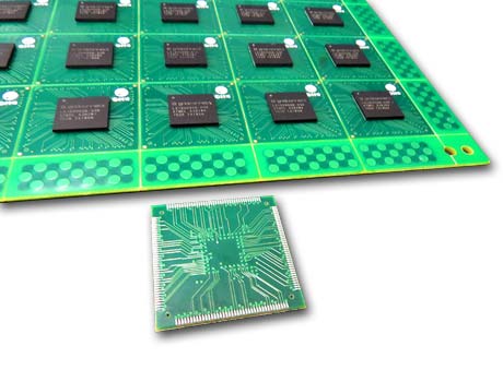
Above is a 180 ball BGA to 160 lead QFP adapter produced in panel form. A six layer PCB was required to convert signals from the original QFP footprint, which consisted of a powerful microprocessor, to the BGA on the top side. The BGA devices were assembled onto a pre-scored PCB, using our in-house SMT assembly line, with solder columns applied to the backside to solder to the original QFP pads. Individual parts were then separated and packaged in trays or tape and reel. The only change incurred for end user was a change of BOM from QFP device to QFP adapter, with no change in in the target board or assembly process.
This dual-supply (1.27mm pitch,24 lead) 8-bit translating transceiver, which interfaces between a 3V and a 5V bus in a mixed 3V/5V environment, was replaced with a new compact form factor (0.65mm pitch, 24 leads) using 1:1 pin mapping. Unique PCB manufacturing technology allows edge plating on the converter PCB to produce side castellations which are easily soldered.
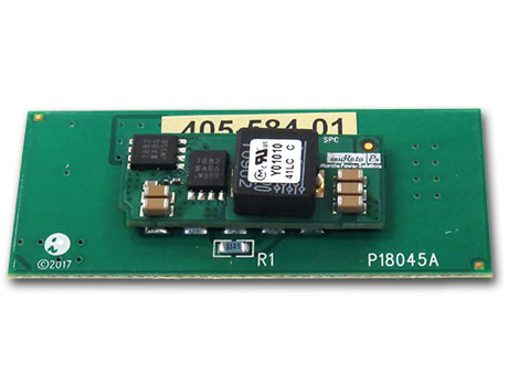
This DC/DC converter includes output voltage trimming. A 2 layer PCB with 2 Oz copper cladding can handle 10 Amp current from the converter. Simply changing a single trim resistor changes the output from 1.5 to 2.5V. Modularity options such as these allow a base device to be mass-produced at very low cost.
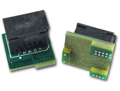
This custom JTAG adapters converts surface mount pads on the development board to test headers for debug cable attachment or firmware updates. The adapter has machined posts to overcome existing components on the target board and connect SMT pads from multiple locations.
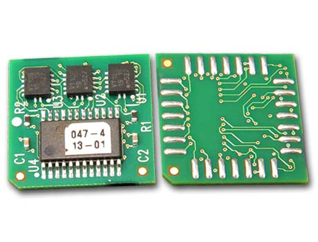
Fix adapter mitigates analog error of driving relay coil current. Original programmable device outputs 4mA at 2.4V, but required 8.4mA, causing it to fail occasionally. A fix adapter was designed to carry a smaller programmable device and high current buffers. The bottom side has solder columns to solder down to existing PLCC footprint. Ironwood provides pre-programming service using Xeltek programmers.
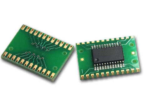
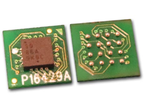
Another example is the conversion of a QFN to BGA device. This PC-QFN16A/BGA16C-01 is mapped specifically for the On Semiconductor multi-function differential Logic Gate NBSG86A. The part consists of a single piece FR4 (High temp PCB) with solder balls on the bottom side which can be easily soldered with SMT techniques.
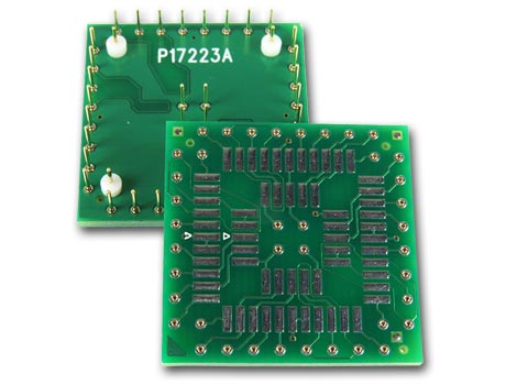
This universal converter for two devices, 20 pin LCC or 40 pin LCC, works with both footprints. Both devices are converted to Pin Grid Array (PGA) on the bottom side. Gold plated male terminal pins are pressed into PCB for a robust interconnection.
When availability or performance of a given IC becomes an issue, using a package converter with substitute device(s), without redesign of the target system, is the most economical solution for both time and cost. Technology advancements such as shaped solder, J-lead, edge castellation, micro blind/buried vias, flex PCB, embedded capacitor/resistor enable adapters to solve any type of constraints faced by end products, in both RoHS or non-RoHS versions.
Simple or complex adapters can easily increase the average component life cycle to align with the end product life cycle of the parent system, which is a must for military and medical applications.
For a specific application, click here to Request a Quote