Probe Socket Configurations
Ironwood Electronics has recently introduced series of high performance BGA socket for high speed probing of the memory chip and processor debugging during the design phase. Figure 1 shows a BGA socket that is designed for 1Gb Mobile DDR2-S4 SDRAM (12x12mm, 0.5mm pitch, 168 FBGA Package). Customer can use this stacked socket to probe 1Gb memory device using Agilent’s Flex Probe stacked inside the socket. Agilent’s probe makes contact with the target PCB through the 0.5mm thick high density elastomer contact. Memory chip sits on top of the Probe and makes contact with it through high speed elastomer contact as well. Agilent’s Probe brings out the signals to oscilloscope/logic analyzer for high speed probing. A list of probe socket available for processor and memory is shown in table 1.

| Ironwood Part Number | Processor | Memory | Bottom to Top Stack up |
| C8453 | BGA841, 12x12mm, 0.4mm pitch, 29×29 full array | BGA168, 12x12mm, 0.5mm pitch, 23×23 partial array | Target PCB > Elastomer > Processor > Elastomer > Memory probe with memory soldered |
| C9133 | N/A | BGA168, 12x12mm, 0.5mm pitch, 23×23 partial array | Target PCB > Elastomer > Memory Probe > Elastomer > Memory |
| C9666 | BGA841, 12x12mm, 0.4mm pitch, 29×29 full array | BGA168, 12x12mm, 0.5mm pitch, 23×23 partial array | Target PCB > Elastomer > Processor Probe with Processor soldered > Elastomer > Memory |
| C10015 | BGA664, 12x12mm, 0.57mm interstitial pitch, 20×20 partial array | BGA216, 12x12mm, 0.4mm pitch, 29×29 partial array | Target PCB > Elastomer > Processor > Spring Pin > Memory probe > Elastomer > Memory |
| C10040* | BGA619, 12x12mm, 0.4mm pitch, 28×28 partial array | N/A | Target PCB > Elastomer > Processor |
| C10062 | BGA520, 12x12mm, 0.4mm pitch, 29×29 partial array | BGA168, 12x12mm, 0.5mm pitch, 23×23 partial array | Target PCB > Spring Pin > Processor > Spring Pin > Memory Probe > Spring Pin > Memory |
| C10919 | BGA617, 12x12mm, 0.4mm pitch, 29×29 partial array | BGA168, 12x12mm, 0.5mm pitch, 23×23 partial array | Target PCB > Elastomer > Processor > Elastomer > Memory probe > Elastomer > Memory |
| C10920 | BGA617, 12x12mm, 0.4mm pitch, 29×29 partial array | BGA216, 12x12mm, 0.4mm pitch, 29×29 partial array | Target PCB > Elastomer > Processor > Elastomer > Memory probe > Elastomer > Memory |
| * To be used with other Probe Sockets | |||
If the configuration listed in table 1 is not suitable for your device, the first step in procuring custom probe socket is that customer communicates their device specification to Ironwood Electronics. An application engineer will be assigned for this request who works with your design engineer and produce a custom probe socket drawing that shows footprint and stack up information. A proposal will be sent to the customer after acceptance of the custom probe socket drawing. We provide various options such as first article, delivery schedule and quantity price break downs. At the start of the project, our application and design engineering team will work on your project and keep customer updated on schedules and project milestones. For your custom packages, please contact 800-404-0204 or email info@ironwoodelectronics.com
Why do you need a Probe Socket?
Evolution from cell phones with only a base-band processor and limited memory to today’s high-end smart phones with an multi-core applications processor and memory has driven the industry to 3-D packaging solutions. 3-D packaging can be achieved via die stacking in one package, package-in-a-package stacking or package on package stacking. Each method has its advantages and disadvantages. Package on package stacking, which has been evolved in a variety of formats, enables stacking of packages from different suppliers and mixed IC technologies. It also allows for burn-in and testing prior to stacking.
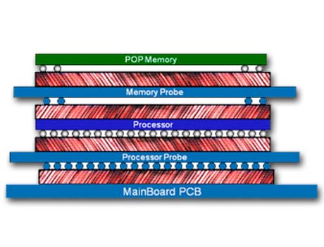
In a stacked package, typically the bottom package is processor and the top package is memory. Because of additional applications required by consumer industry, IC engineers add more features to their 2nd generation processor and the memory performance is increased by faster communication to the processor. Test engineers need a socket which can test 1st generation processor and memory. We have seen many product offerings for this one level stacked socket. In order to move from 1st generation to 2nd generation devices, a test engineer needs 2, 3, or 4 level stacked socket. During development, test engineer needs to use a processor probe in between processor and the main development board to connect with logic analyzer to perform the signal capability functions. Then test engineer uses memory probe in between the memory and processor to verify the performance of newer memory. The picture (Figure 2) below shows a typical four level interconnect enabling development sequence of 3D ICs. Designing a socket to accommodate these variations bring many challenges. In this article, two major challenges are addressed.
Force Challenges
The biggest of all challenge is force balancing. In a simple case, processor has 515 solder balls and the PoP (Package on Package) memory has 168 solder balls. Memory with 168 balls requires 5 lbs of force for optimum compression that results in less than 20 milliohms contact resistance per ball. Processor with 515 balls requires 15 lbs of force for optimum compression that results in less than 20 milliohms contact resistance per ball. In order to balance the force at each level, another 10 lbs of force is needed at the memory level. This will balance the force at processor level. When 15 lbs of force is applied to the memory with only 168 balls, the elastomer underneath memory will be over compressed. Also, there is potential of memory device warpage due to high force. To counter balance, a sheet of rubber whose thickness can fill the gap between bottom side of memory device and top side of elastomer interface has been used. This rubber can absorb the extra 10 lbs of force resulting only recommended force on the elastomer section that was interfaced with memory device. Similar force balancing has to be accomplished at each level of interconnection if force variation exists.
Alignment Challenges
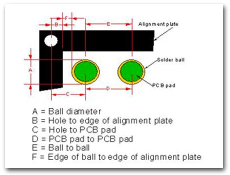
Similar to force balancing, alignment level challenges has been addressed at each interconnection level. Let us consider a simple case where a test engineer needs to test processor only. It is a simple one level interconnection. The following (Figure 3) picture shows typical variations in XY direction for a single stack up interconnect.
Elastomer is the “interconnect” used in this stack up. Top side of the elastomer interfaces with device ball and brings the electrical signal down to test board. Elastomer consists of gold plate brass wires embedded in silicone rubber. In order to have least resistance electrical path, greater than 50% of area with respect to pad/ball dimension to be made contact with top and bottom side. To ensure proper alignment, all the components are precisely positioned with one datum (alignment pin). The following scenario shows worst case situation.
| PCB Alignment Hole position | +0.025mm |
| Ball guide Alignment Hole position | +0.025mm |
| PCB Pad location/Size | +0.05mm |
| Total | 0.1mm off from nominal location |
With 0.24mm minimum pad diameter for 0.4mm pitch BGA, elastomer contacts more than 58% of the pad with 0.1mm off from nominal location. This means pin alignment hole and ball alignment hole has to be manufactured with very tight tolerance ±0.025mm. This XY variation occurs on each level of the stack up. All the levels should ensure greater than 50% contact coverage area for the best electrical connection. Similar calculations have to be made for Z variations and manufacturing tolerances has to be updated such that >50% of pad is covered by elastomer. Alternatively, if spring pins are used instead of embedded wire elastomer for interconnect options; the alignment challenge increases two fold. First, we have to add spring pin diameter tolerance. Second, we have to add the hole tolerance that positions the spring pin. In order to ensure proper electrical connection, manufacturing tolerances have to be very tightly controlled on these two additional factors which results in yield issues and high cost. Selecting appropriate interconnect medium plays major role in development cost.
Pitch, pin count and performance complexities in 3D packages are driven to its extreme due to consumer demand. Simple two level IC stacking requires four level interconnection for development needs. XYZ alignment challenges at each interconnect level push manufacturing capabilities to the level never seen before. Force balancing at each level requires innovative design and new materials with unique properties.
For more information, please contact Ironwood Electronics application engineers at 800-404-0204 or info@ironwoodelectronics.com