Universal BGA Socket for eMMC
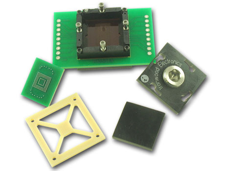
Ironwood Electronics has recently introduced universal high performance BGA socket for high speed testing of the memory devices during the design and application development phase. Figure 1 shows a universal BGA socket that is designed for all eMMC Packages from major memory vendors such as Samsung, Hynix, Toshiba, Sandisk, Micron, etc.
What is eMMC?
eMMC acronym for Embedded Multi Media Card describes an architecture consisting of an embedded storage solution with MMC interface, flash memory and controller, all in a small ball grid array(BGA) package. These eMMC memory devices cover a wide area of applications such as smart phones, cameras, tablet computers, digital recorders, MP3 players, electronic toys, etc. that needs high mobility and high performance at a low cost. Other features include low power consumption and high data throughput at the memory card interface. According to iSuppli research, the evolution of eMMC has been fast with phenomenal enhancements to performance. eMMC 4.5 specifically addresses several new capabilities such as increased longevity, doubling memory transfer speeds, addition of volatile cache enabling faster performance, etc. This means testing these eMMC devices can be possible only by using high speed interconnects.
GHz BGA Socket
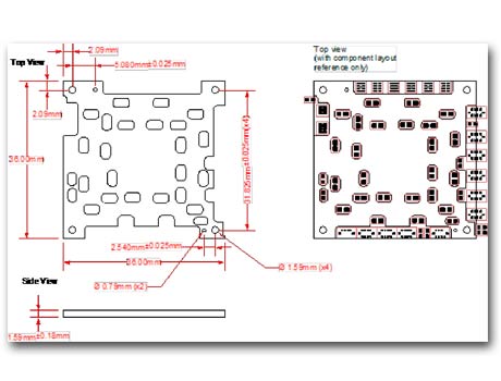
The SG-BGA-7219 universal BGA socket is designed for testing eMMC BGA device and operates at bandwidths up to 10 GHz with less than 1dB of insertion loss. The contact resistance is typically 20 milliohms per pin. The BGA socket connects all pins with 10 GHz bandwidth on all connections. The BGA socket is mounted using supplied hardware on the target PCB with no soldering, and uses smallest footprint in the industry. The BGA socket also incorporates a new quick insertion method using shoulder screws and swivel socket lid so that IC’s can be changed out quickly. The BGA socket also features floating compression mechanism to accommodate package manufacturing variations. The application of the BGA socket is to verify the function of eMMC device that provides a flexible, industry-standard architecture that simplifies mass storage designs for portable consumer electronics products based upon the industry-standard MMC System Specification v4.5 and JEDEC MO-276 BGA packaging standards. The specific package size accommodated by the BGA socket is shown in the table.
The SG-BGA-7219 BGA socket is constructed with high performance and low inductance gold plated embedded wire on elastomer as interconnect material between device and PCB. The elastomer used for high-density application consists of an ultra fine pitch matrix (0.05mm x 0.05mm) of gold plated wires (20 micron diameter), which are embedded at a 63-degree angle in a soft insulating sheet of silicone rubber. The gold-plated brass filaments protrude several microns from the top and bottom surfaces of the silicone sheet. Solder balls from the IC package come in contact with the top end of elastomer wire. The bottom end of elastomer wire contacts the circuit board pad and thereby makes an electrical path for the signal. The number of wire filaments making contact depends on the solder ball and circuit board pad diameters. In SG-BGA-7219, minimum 4 wires and maximum 16 wires will connect solder ball to PCB pad. The GHz BGA socket testing can be summarized as a mechanism in which a downward force applied to an IC compresses its solder balls onto an elastomer, which in turn compresses on the circuit board, thereby making electrical connection. The insulation resistance between connections with 500V DC is 1000 M. The temperature range is -35C to +100 C. The pin self inductance is 0.15 nH and mutual inductance of 0.025 nH. Capacitance to ground is 0.01 pF. Current capacity is 2 amps per pin.
| Vendor | eMMC Packages |
| Hynix | FBGA169 12×16 FBGA169 14×18 FBGA153 11×10 FBGA153 11.5×13 |
| Samsung | FBGA169 12×16 FBGA169 14×18 FBGA169 12×18 FBGA153 11.5×13 |
| Toshiba | JEDEC MO-276 |
| Sandisk | FBGA169 12×16 FBGA169 14×18 FBGA153 11.5×13 |
| Micron | JEDEC MO-276 |
SG-BGA-7219 GHz BGA socket requires a backing plate to prevent the deflection of the target circuit board due to high downward force. If the backside of target PCB contains capacitors and resistors, a custom insulation plate with cavities milled for those capacitors and resistors can be designed. The insulation plate sandwiches between the backing plate and the target PCB. Figure 2 is an example of an insulation plate.
Assembly and testing of BGA socket is explained in the video.
Pitch, pin count and performance complexities in BGA memory packages are driven to its extreme due to consumer demand. Testing these BGA memory packages to its rated performance can be accomplished by high speed BGA socket interconnect with precise XYZ alignment that pushed manufacturing capabilities to the level never seen before.
For more information, please contact Ironwood Electronics application engineers at 800-404-0204 or info@ironwoodelectronics.com